Guangzhou Minder-Hightech Co.,Ltd.

Home
About Us
MH Equipment
Solution
Oversea Users
Video
Contact Us
Home> Ultrasonic Inspection System
  • MDHWS321 Ultrasonic Inspection System Scanning Acoustic Microscope
  • MDHWS321 Ultrasonic Inspection System Scanning Acoustic Microscope
  • MDHWS321 Ultrasonic Inspection System Scanning Acoustic Microscope
  • MDHWS321 Ultrasonic Inspection System Scanning Acoustic Microscope
  • MDHWS321 Ultrasonic Inspection System Scanning Acoustic Microscope
  • MDHWS321 Ultrasonic Inspection System Scanning Acoustic Microscope
  • MDHWS321 Ultrasonic Inspection System Scanning Acoustic Microscope
  • MDHWS321 Ultrasonic Inspection System Scanning Acoustic Microscope

MDHWS321 Ultrasonic Inspection System Scanning Acoustic Microscope

Product Description

MDHWS321 Ultrasonic Scanning Acoustic Microscope

MDHWS321series ultrasonic scanning microscope is a non-destructive testing imaging equipment suitable for semiconductor industry. It mainly uses high frequency ultrasound to detect all kinds of semiconductor devices and materials, and can detect defect such as pores, cracks, inclusions and delamination inside samples, and display them in agraphical way. During the scanning process, it
will not cause damage to the sample and will not affect the performance of the sample.
Feature
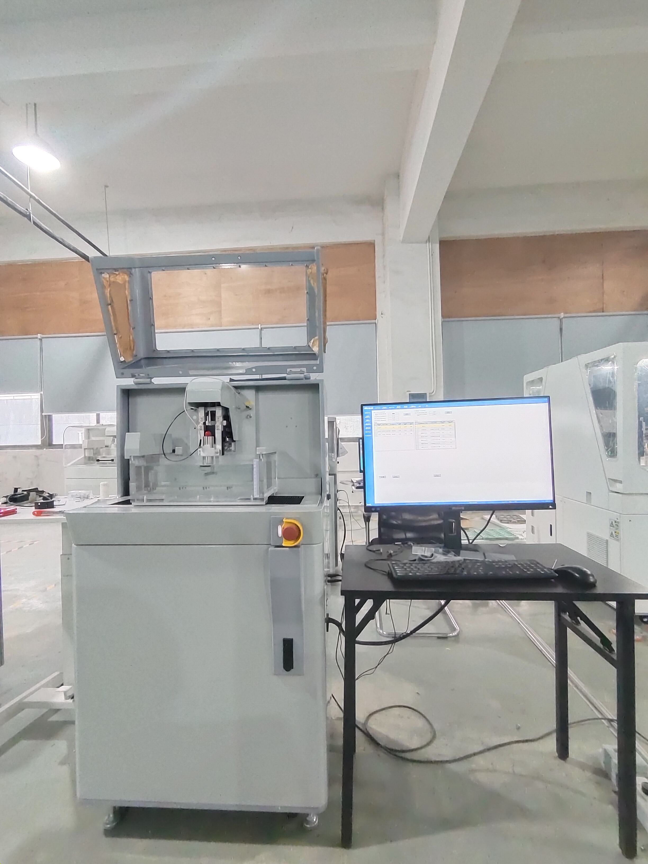
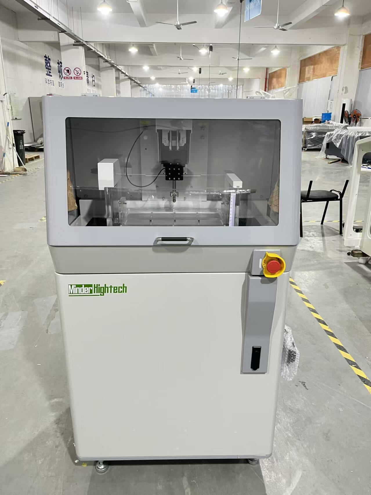
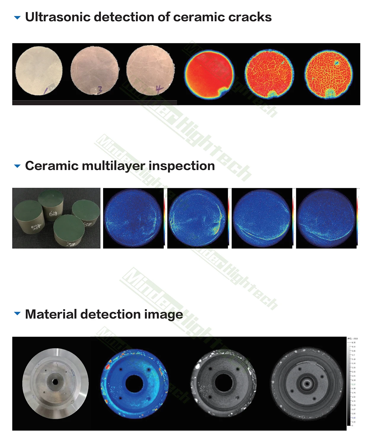
1. With A scan, B scan, C scan, multi-layer scanning, transmission scanning (need to configure transmission scanning unit and receiving probe options), multi-layer scanning, tray-tray scanning, thickness measurement andother series of scanning modes.
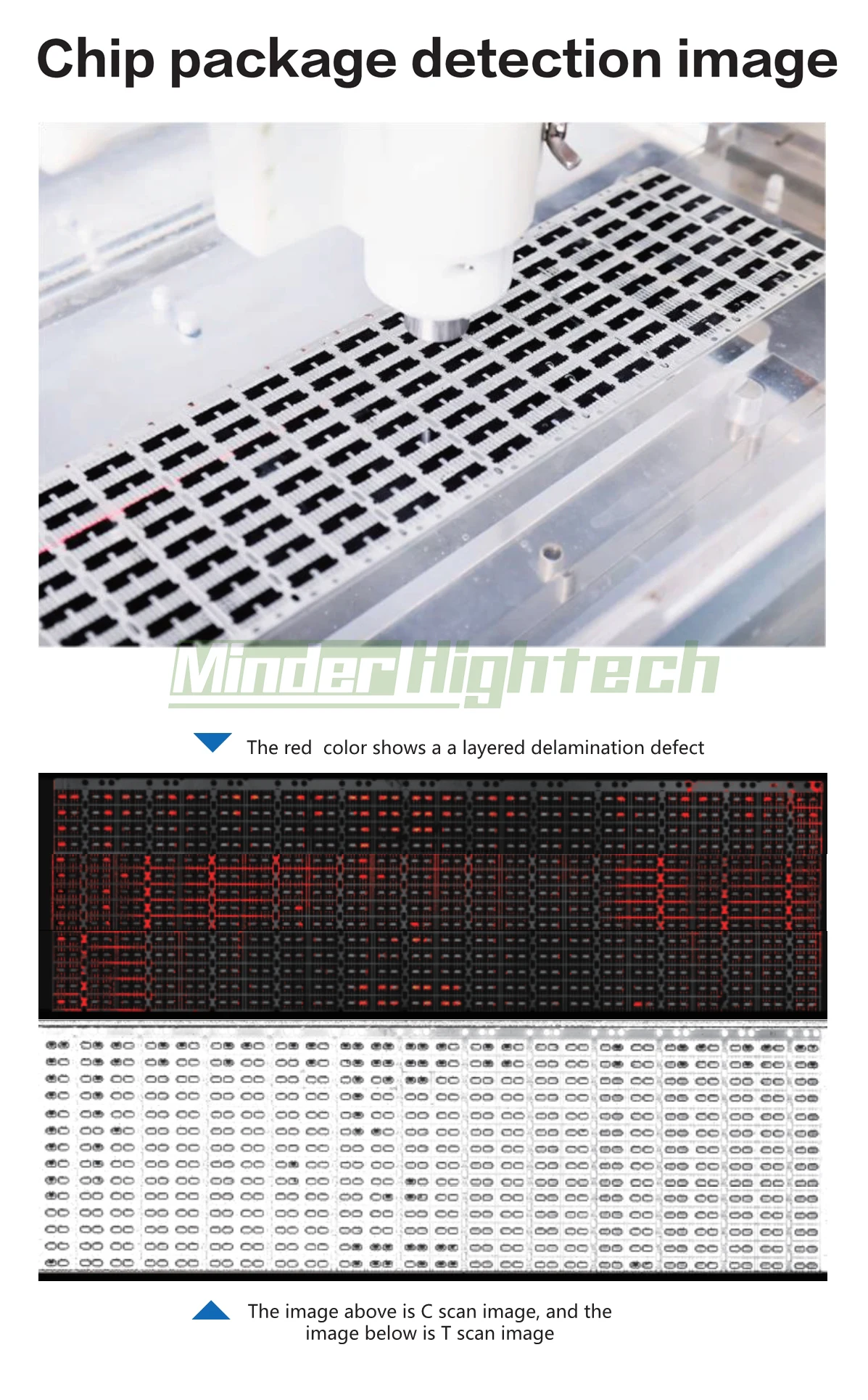
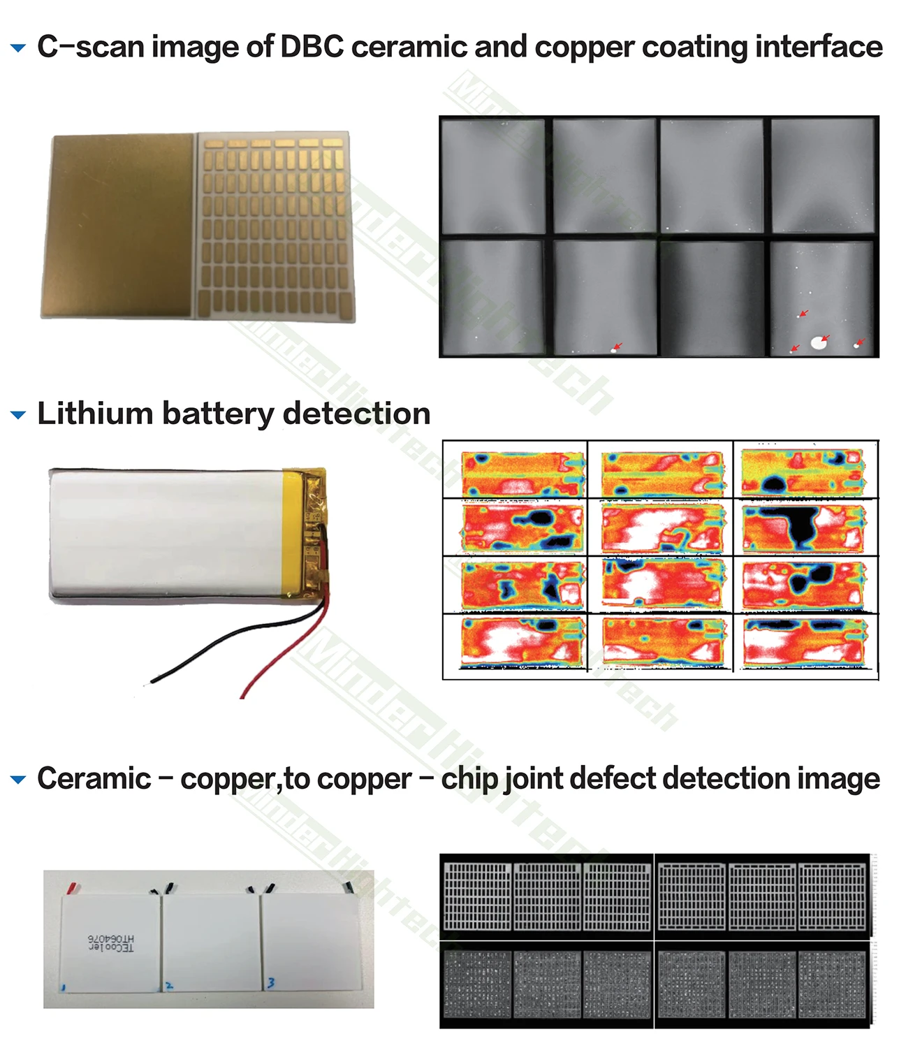
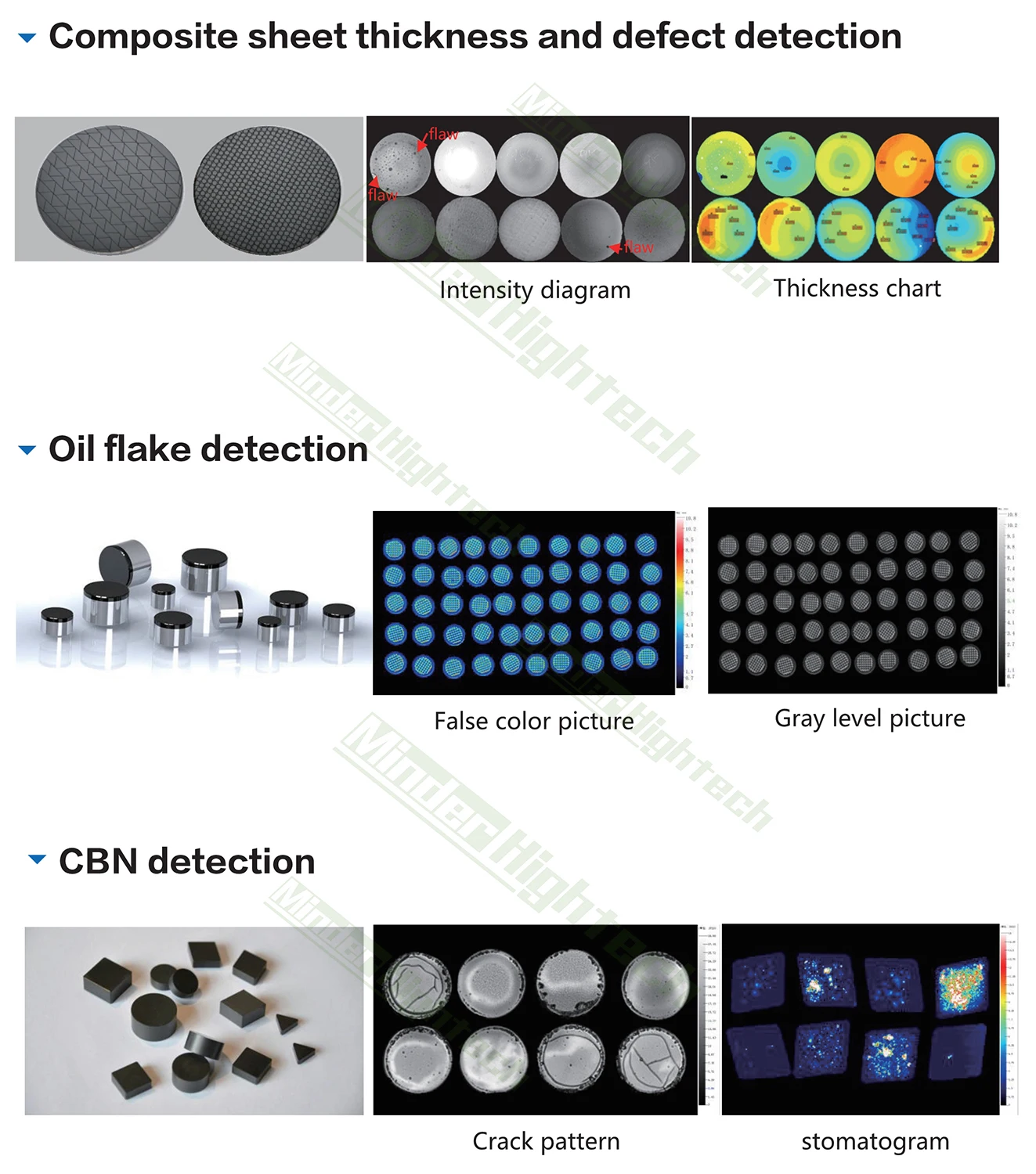
2. With quantitative measurement and analysis function, visually display the position, shape and size of the intemal defects of the tested parts in the form of images, and carry out the size and area statistics of the defects, and automatically calculate the percentage of defects in the measured area; With defect size identification: Thickness and ranging functions
3. With image coloring function, can automatically color according to phase reversal; Manual coloring according to gray level. Automatic coloring according to thickness changes
4. Suitable for the rapid scanning analysis of a single device, can also be placed in batches of samples synchronous defect identification, quickly screen out unqualified products.
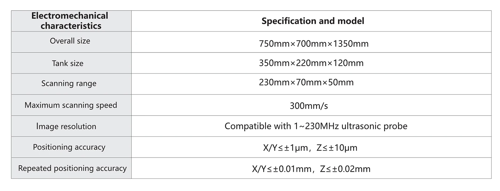
5. Compatible with 1-230MHz ultrasonic probe.
6. Testing software independent research and development, English and Chinese interface, can be continuously upgraded according to customer needs.
Specification
Applications
Suitable for plastic sealed lC, photoelectric device, microwave power device, MEMS device, flip chip, Stacked Die, MCM multi-chip module, diamond composite sheet, electrical welding parts, ceramic materials and other fields of defect analysis.
Packing & Delivery
Company Profile
FAQ
1. About Price:
All of our prices are competitive and negotiable. The price varies depending on the configuration and customization complexity of your device.

2. About Sample:
We can provide sample production services for you, but you may provide some fees.

3. About Payment:
After the plan is confirmed, you need to pay us a deposit first, and the factory will start preparing the goods. After the
equipment is ready and you pay the balance, we will ship it.

4. About Delivery:
After the equipment manufacturing is completed, we will send you the acceptance video, and you can also come to the site to inspect the equipment.

5. Installation and Debugging:
After the equipment arrives at your factory, we can dispatch engineers to install and debug the equipment. We will provide you with a separate quotation for this service fee.

6. About Warranty:
Our equipment has a 12-month warranty period. After the warranty period, if any parts are damaged and need to be replaced, we will only charge the cost price.

Inquiry

Inquiry Email WhatsApp WeChat
Top
×

Get in touch