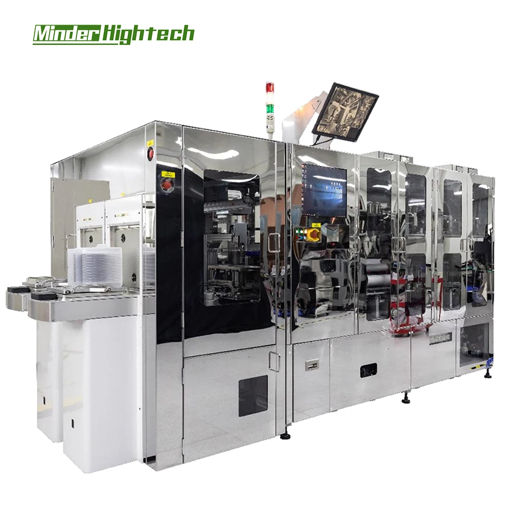
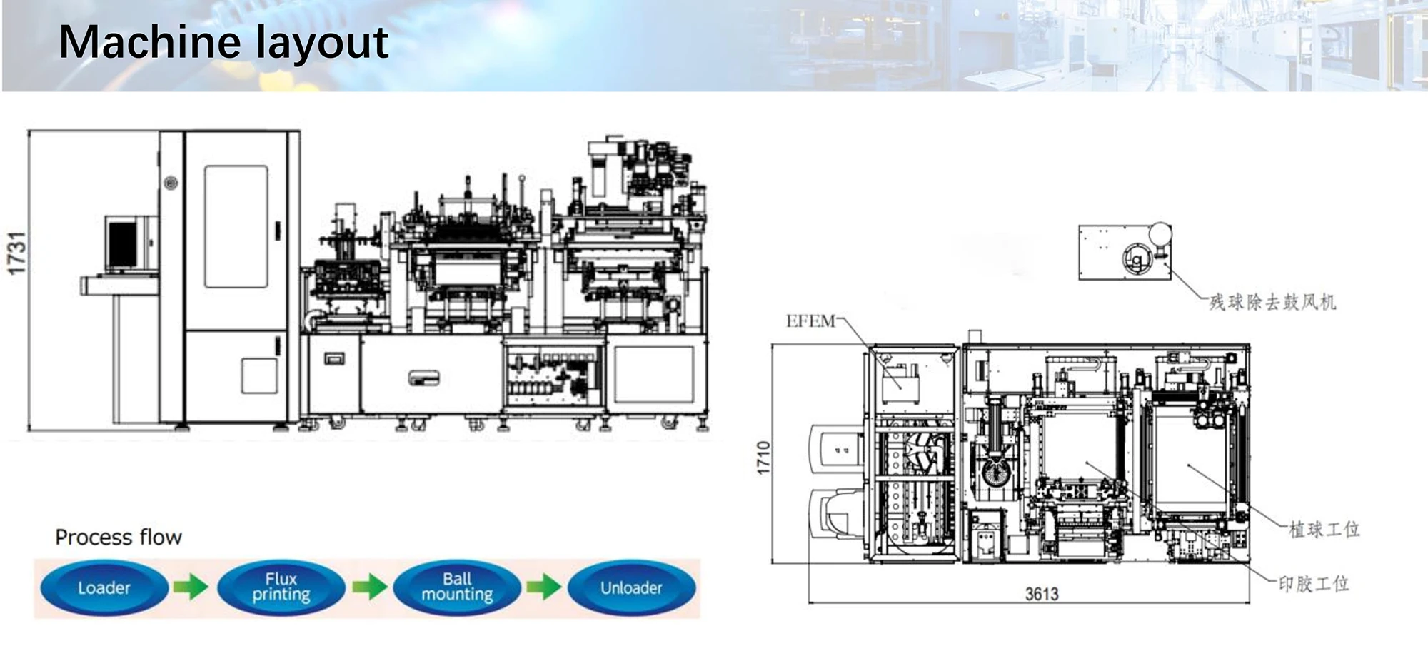
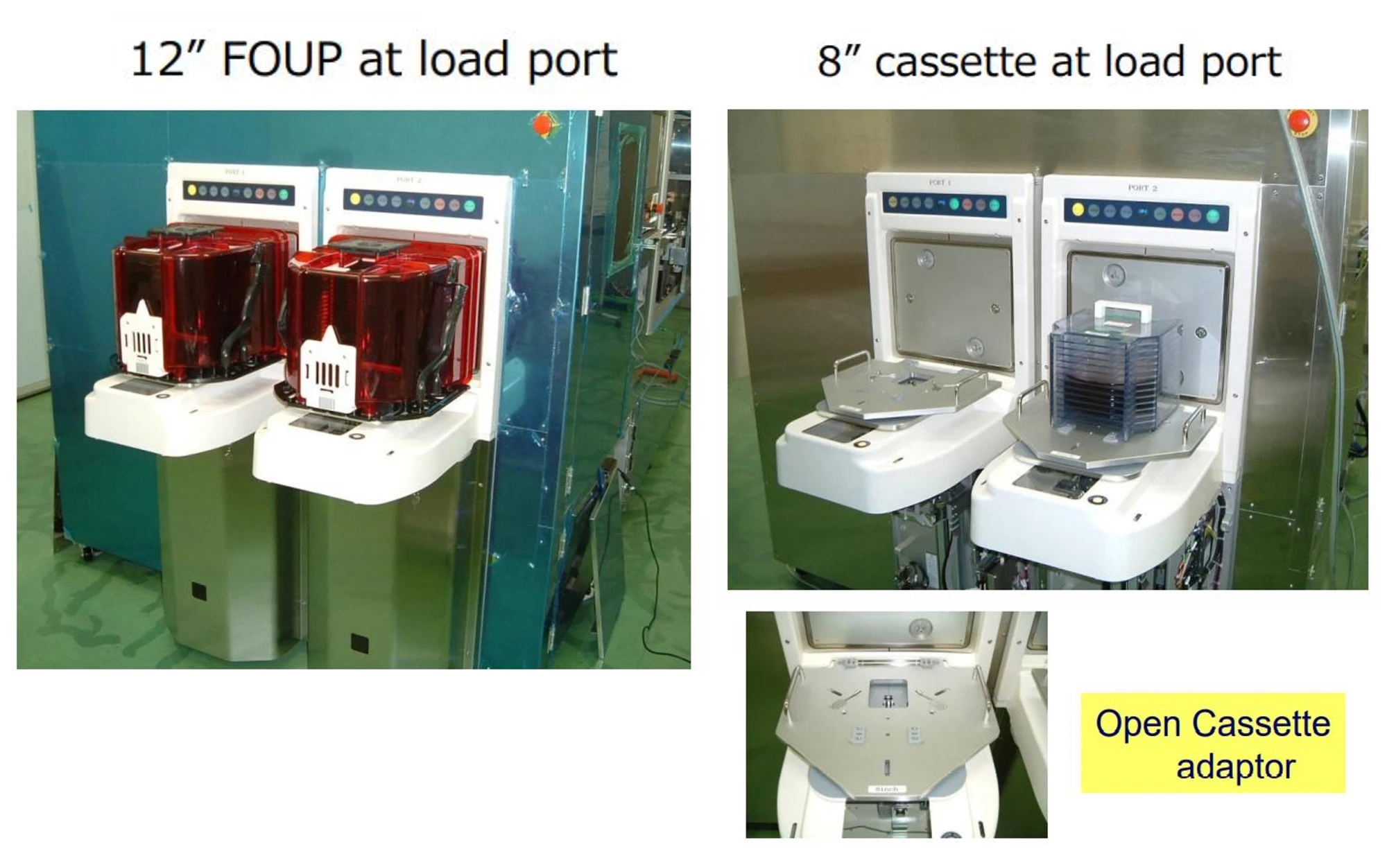
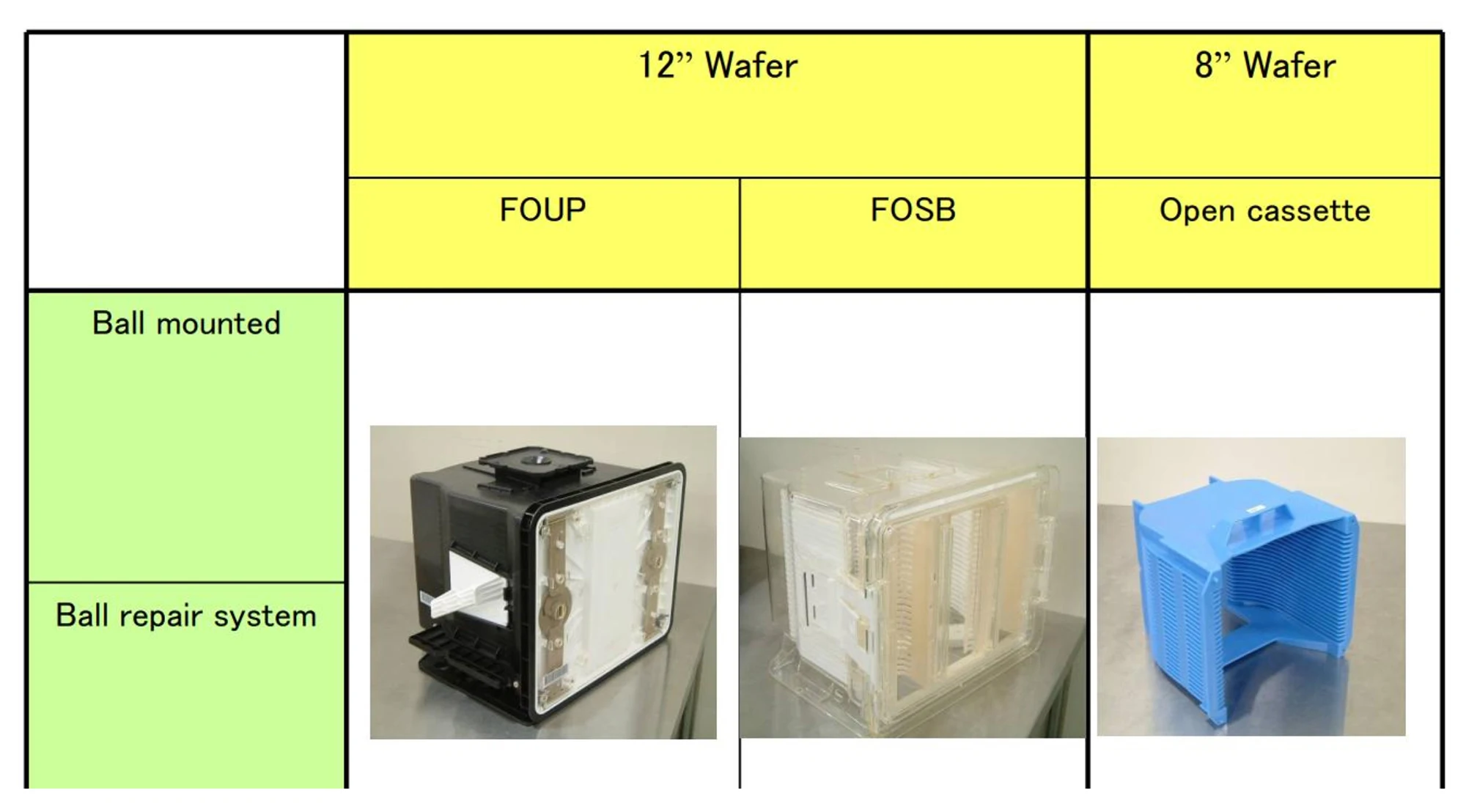
1. Applicable wafer: 12’’ wafer & 8’’ wafer
2. Ball size: ф60[um]~ ф760 [um]、ф30 [um] in Lab test level
3. Wafer Bump:
a). Min. Bump pitch: 100 [um]
b). Min. Bump pad size: 85 [um]
c). Max. Bump count: 2.2KK [pins]
*The data is subject to device conditions
4. 12” Wafer case:
a). Min. Thickness: 200[μm]、100[μm] under lab test level
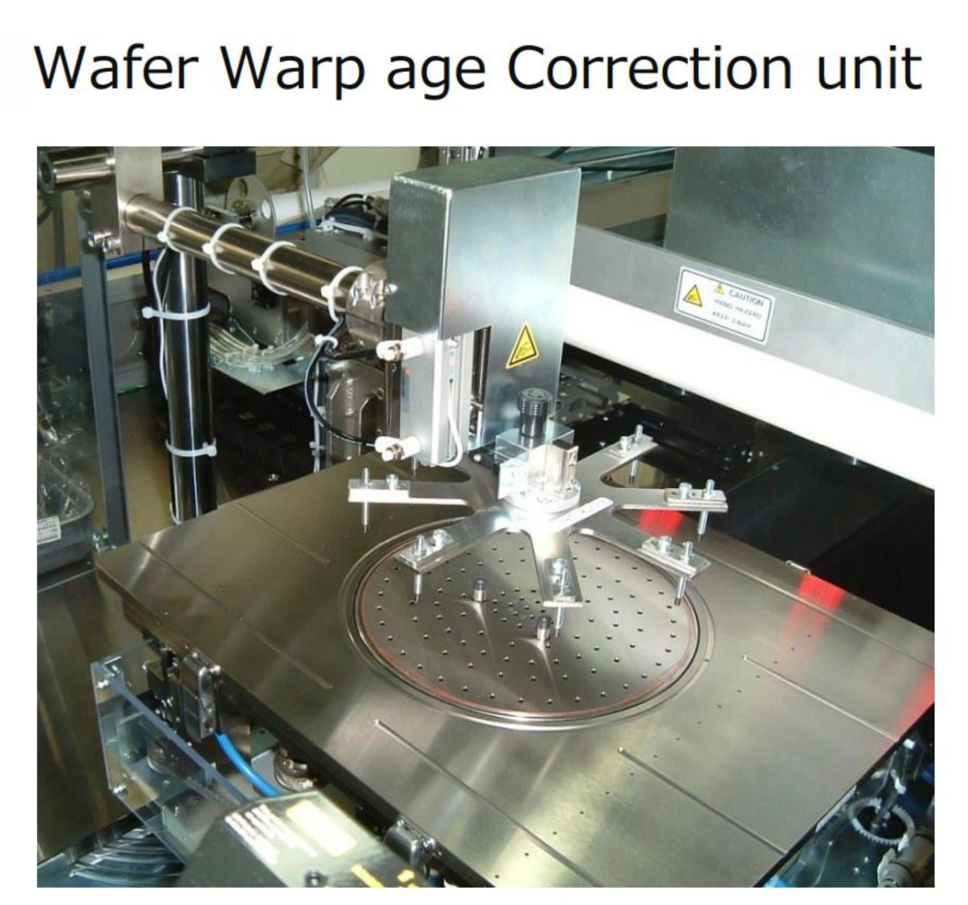
b). Max Warpage Tolerance:6 [mm]/凹case、3 [mm]/凸case
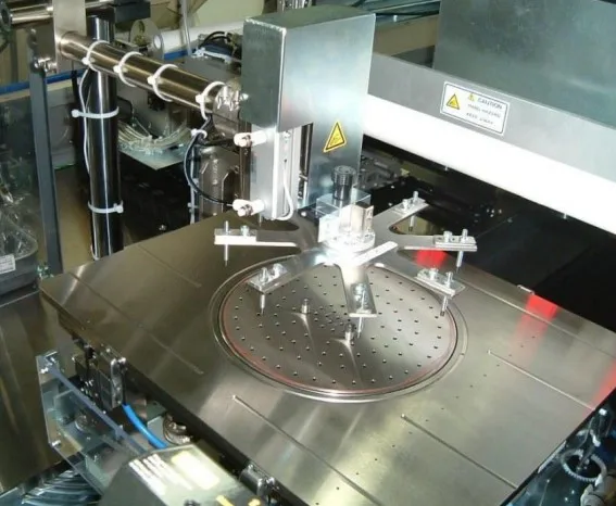
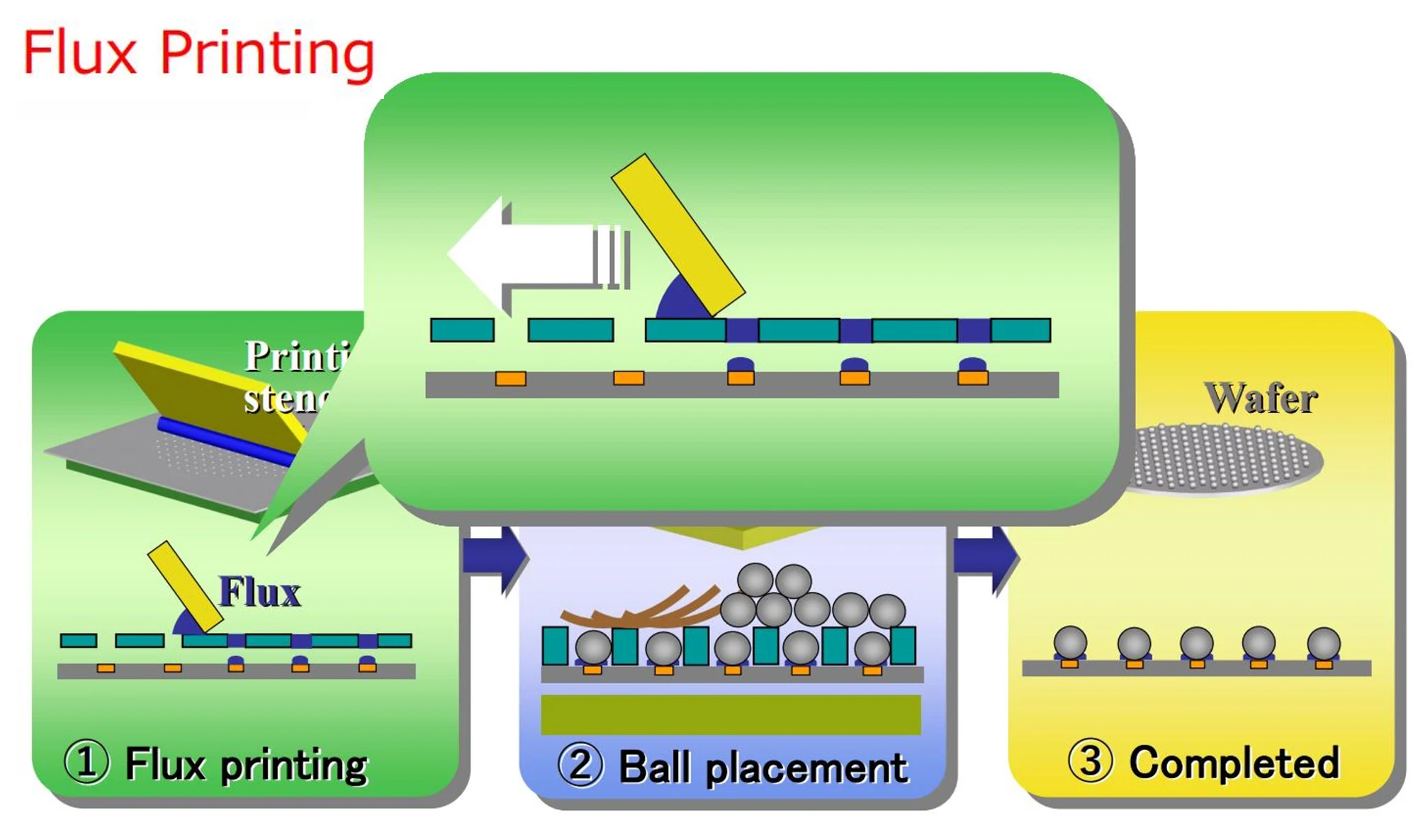
5. Ball mounting Ability
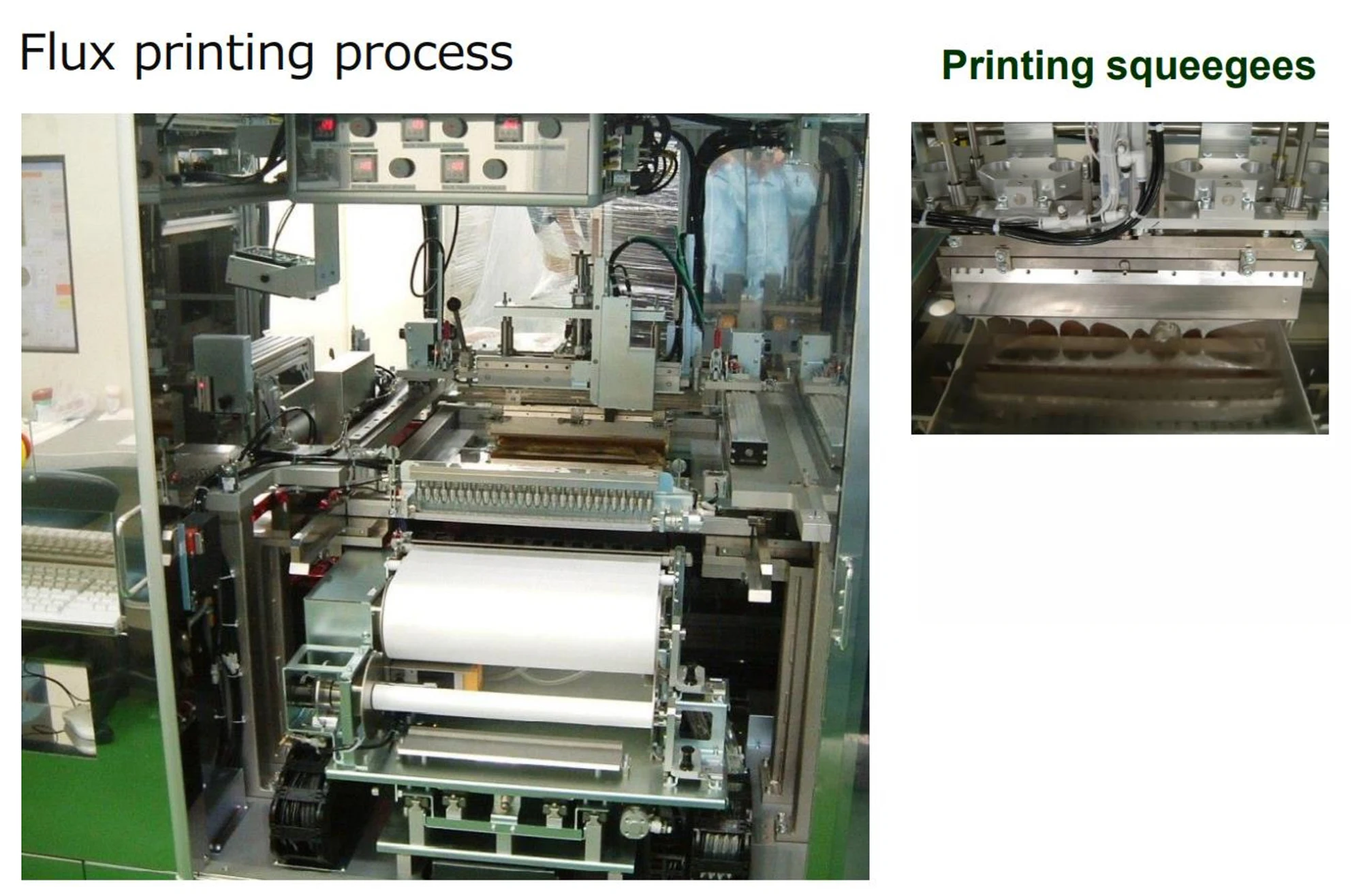
a). Flux Printing Accuracy
Over ф75[um] Ball: +25[um]
Less than ф75[μml Ball: +1/3 of ball diameter
b). Ball mounting Accuracy
Over ф75[um] Ball::±25[um]
Less than ф75[μml Ball: +1/3 of ball diameter
For special case, we can achieve:+13μm
c). Ball Mounting NG Ratio: Less than 30 [ppm]


 EN
EN
 AR
AR
 BG
BG
 CS
CS
 DA
DA
 NL
NL
 FI
FI
 FR
FR
 DE
DE
 EL
EL
 IT
IT
 KO
KO
 NO
NO
 PL
PL
 PT
PT
 RO
RO
 RU
RU
 ES
ES
 SV
SV
 TL
TL
 IW
IW
 ID
ID
 LT
LT
 SR
SR
 SL
SL
 UK
UK
 VI
VI
 ET
ET
 HU
HU
 TH
TH
 TR
TR
 FA
FA
 AF
AF
 MS
MS
 GA
GA
 IS
IS
 HY
HY
 AZ
AZ
 KA
KA