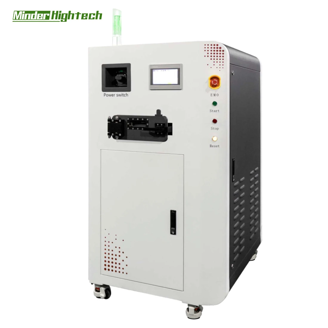


PLASMA source | RF | ||
Power | ICP | _ | |
BIAS | 1000W(option) | ||
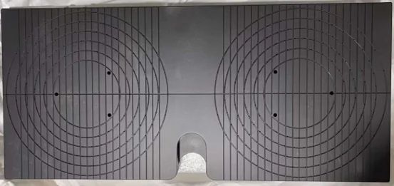
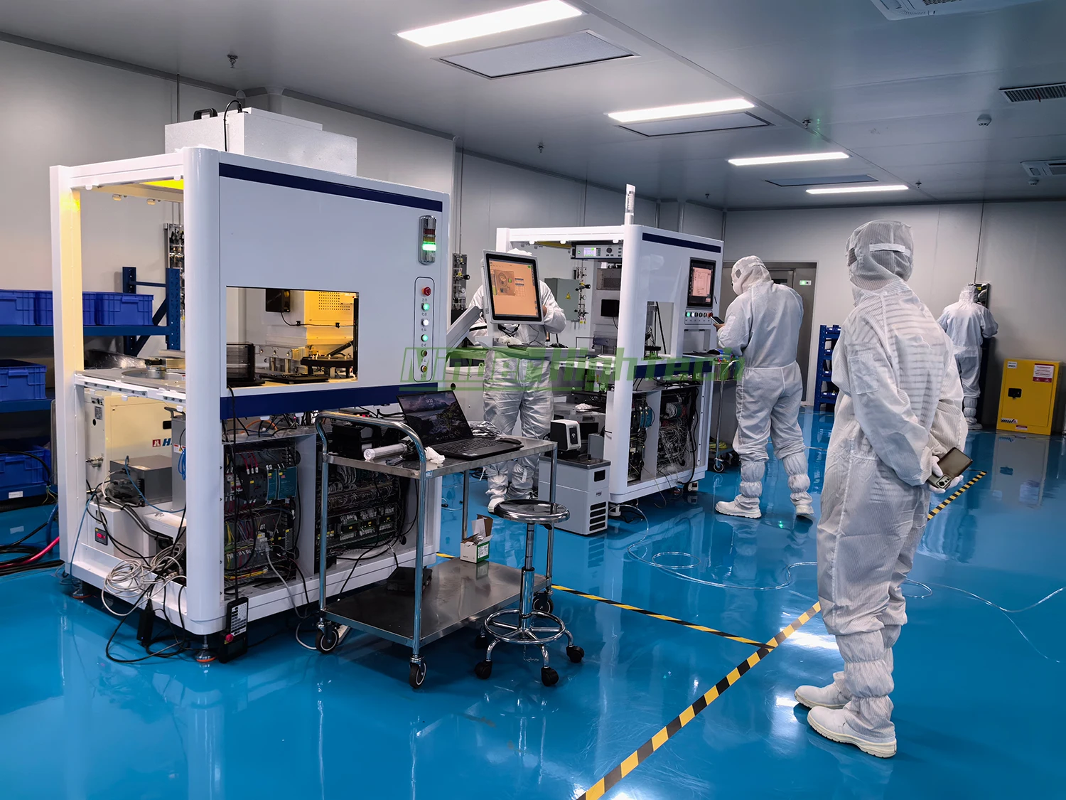
Applicable scope | 4~8 inch | ||
Single processing slice count | 1 | ||
Appearance dimensions | 850mmx900mmx1850mm | ||
System control | PLC | ||
Automation level | Manual | ||
Hardware Capability | ||
Uptime/Available time | ≧95% | |
Mean time to clean (MTTC) | ≦6 hours | |
Mean time to repair(MTTR) | ≦4 hours | |
Mean time between failures(MTBF) | ≧350 hours | |
Mean time between assistant(MTBA) | ≧24 hours | |
Mean wafer between broken(MWBB) | ≦1 in 10,000 wafers | |
Heating plate control | 50-250° | |


Guangzhou Minder-Hightech Co.,Ltd.
Copyright © Guangzhou Minder-Hightech Co.,Ltd. All Rights Reserved
 EN
EN
 AR
AR
 BG
BG
 CS
CS
 DA
DA
 NL
NL
 FI
FI
 FR
FR
 DE
DE
 EL
EL
 IT
IT
 KO
KO
 NO
NO
 PL
PL
 PT
PT
 RO
RO
 RU
RU
 ES
ES
 SV
SV
 TL
TL
 IW
IW
 ID
ID
 LT
LT
 SR
SR
 SL
SL
 UK
UK
 VI
VI
 ET
ET
 HU
HU
 TH
TH
 TR
TR
 FA
FA
 AF
AF
 MS
MS
 GA
GA
 IS
IS
 HY
HY
 AZ
AZ
 KA
KA