Why do semiconductor wafers need to remove photoresist ?
In semiconductor production processes, a large amount of photoresist is used to transfer circuit board graphics through the sensitivity and development of the mask and photoresist to the wafer photoresist, forming specific photoresist graphics on the wafer surface. Then, under the protection of the photoresist, pattern etching or ion implantation is completed on the lower film or wafer substrate, and the original photoresist is completely removed.
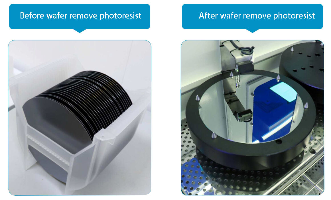
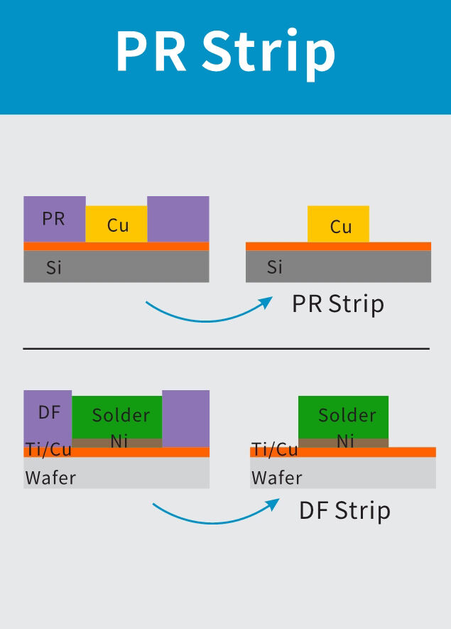
Removing photoresist is the final step in the photolithography process. After the completion of graphic processes such as etching/ion implantation, the remaining photoresist on the wafer surface has completed the functions of pattern transfer and protective layer, and complete removal through photoresist removal process.
The removal of photoresist is a very important step in the microfabrication process. Whether the photoresist is completely removed and whether it causes damage to the wafer will directly affect the subsequent integrated circuit chip manufacturing process.
What are the processes for removing semiconductor photoresist?
Except for the difference in photoresist media, it can be divided into two categories: oxidation removal and solvent removal.
Comparison of various adhesive removal methods:
|
Photoresist removal method
|
Oxidation removal of photoresist
|
Dry removal of photoresist
|
Solvent removal of photoresist
|
|
Main principles |
The strong oxidizing properties of H ₂ SO ₄/H ₂ O ₂ oxidize the main components C and H in photoresist to C0 ₂/H ₂ 0 ₂, thereby achieving the purpose of debonding |
Plasma ionization of 0 ₂ forms free 0, which has strong activity and combines with C in the photoresist to form C0 ₂. C0 is extracted by the vacuum system |
Special solvents swell and decompose polymers, dissolve them in the solvent, and achieve the purpose of degumming |
|
Main application areas |
Perishable metal, therefore not suitable for degumming in AI/Cu and other processes |
Suitable for the vast majority of debonding processes |
Suitable for debonding process after metal processing |
|
Main advantages |
The process is relatively simple |
Completely remove photoresist, fast speed |
The process is relatively simple |
|
Main Disadvantages |
Incomplete removal of photoresist, inappropriate process, and slow debonding speed |
Easy to be contaminated by reaction residues |
Incomplete removal of photoresist, inappropriate process, and slow debonding speed |
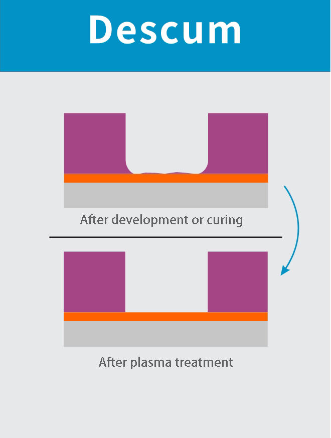
As can be seen from the above figure, dry debonding is suitable for most debonding processes, with thorough and fast debonding, making it the best method among existing debonding processes. Microwave PLASMA debonding technology is also a type of dry debonding.
Our microwave PLASMA removes photoresal glue equipment, equipped with the first domestic microwave semiconductor photoresal removal generator technology, configures the magnetic flow rotation rack to make the microwave plasma more efficient and uniform output. Silicon wafers and other metal devices provide "microwave+bias RF" dual power technology to meet the needs of different customers.
Microwave PLASMA Remove photoresist machine
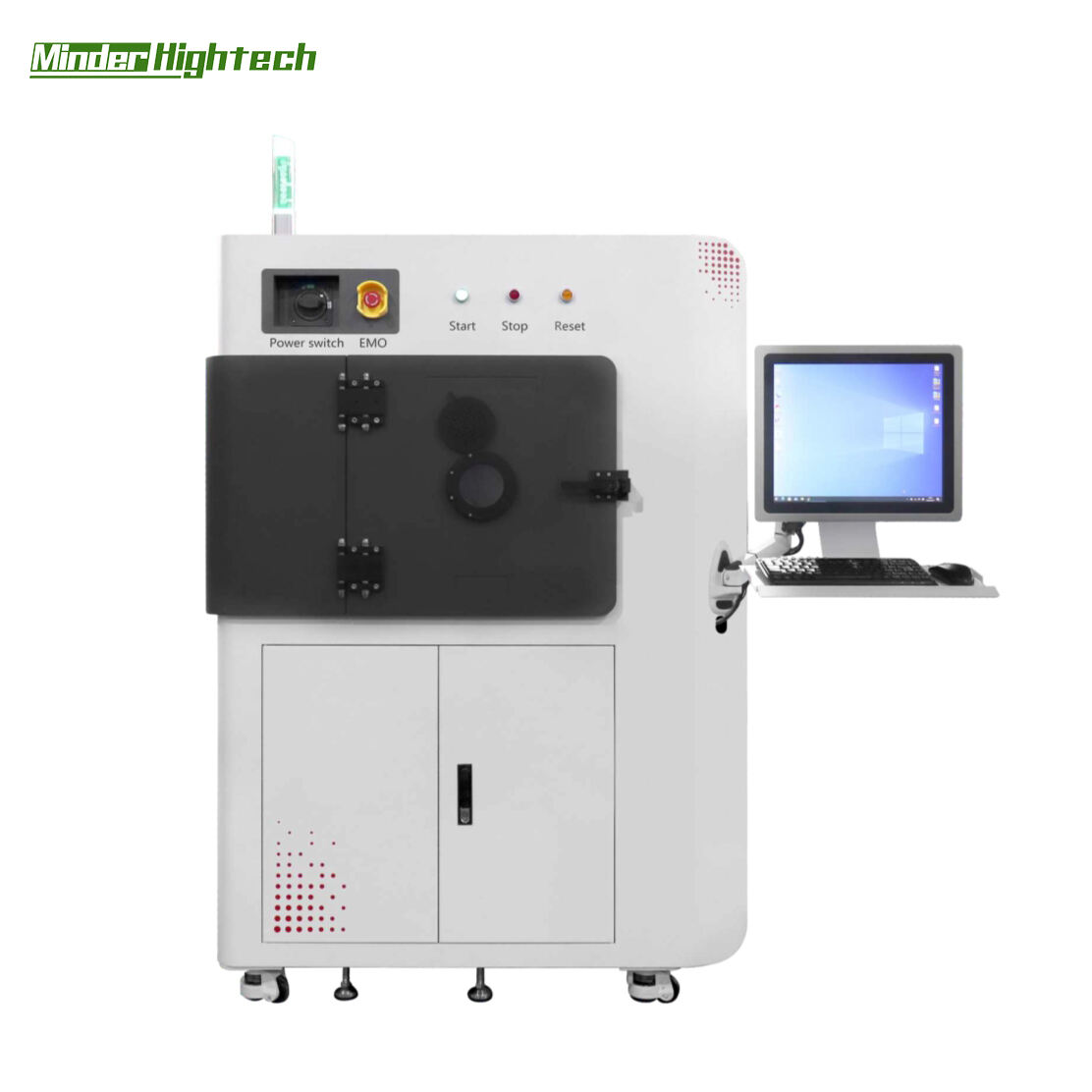
① The plasma of free radical molecules has no bias and no electrical damage;
② The product can be placed on pallets, slotted or enclosed Magizine, with high processing efficiency;
③ Magizine can be configured with a rotating frame, and through reasonable ECR design and good gas flow regulation, it can achieve relatively high uniformity;
④ Integrated control system design, patented control software, more convenient operation;

Guangzhou Minder-Hightech Co.,Ltd.
Copyright © Guangzhou Minder-Hightech Co.,Ltd. All Rights Reserved
 EN
EN
 AR
AR
 BG
BG
 CS
CS
 DA
DA
 NL
NL
 FI
FI
 FR
FR
 DE
DE
 EL
EL
 IT
IT
 KO
KO
 NO
NO
 PL
PL
 PT
PT
 RO
RO
 RU
RU
 ES
ES
 SV
SV
 TL
TL
 IW
IW
 ID
ID
 LT
LT
 SR
SR
 SL
SL
 UK
UK
 VI
VI
 ET
ET
 HU
HU
 TH
TH
 TR
TR
 FA
FA
 AF
AF
 MS
MS
 GA
GA
 IS
IS
 HY
HY
 AZ
AZ
 KA
KA


