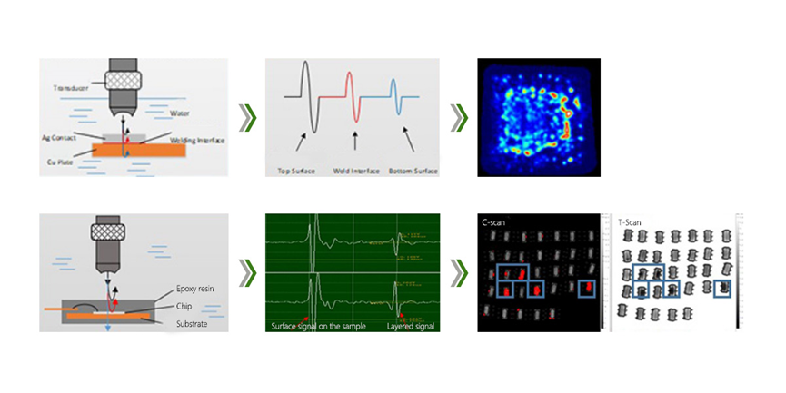
Ultrasonic Testing Principle
Ultrasonic transducer generates ultrasonic pulse which reaches DUT through the coupling medium (water).
Due to the difference of acoustic impedance, ultrasonic wave reflect at the interface of different materials.
Ultrasonic transducer receives the reflected echo and converts it to electrical signals.
Computer processes the electrical signal and display waveform or image.
Scanning form
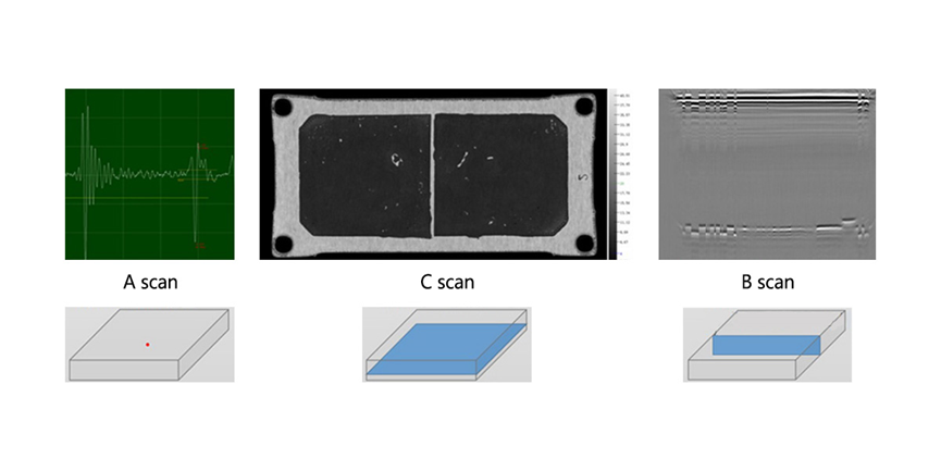
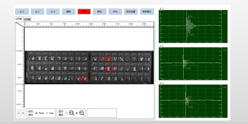
A scan: waveform at a certain point;
The horizontal axis indicates the time when the waveform appears;
The vertical axis indicates the waveform amplitude.
C scan: transverse cross-sectional scan;
The horizontal and vertical axes indicate the physical dimensions;
The color indicates the waveform amplitude.
B scan: longitudinal cross-sectional scan;
The horizontal axis indicates the physical dimensions;
The vertical axis indicates the time when the waveform appears;
The color indicates the waveform amplitude and phase
Multi-layer scanning: multi-layer C scanning is performed in the depth direction of the sample.

Transmission scanning: receivers are added to the bottom of the sample to collect the transmitted sound waves to generate images.
Advantages and limitations of detection
Advantages:
1. Ultrasonic detection is applicable to a wide range of materials, including metals, non-metals, and composite materials;
2. It can penetrate most materials;
3. It is very sensitive to interface changes;
4. It is harmless to the human body and the environment.
Limitations:
1. The waveform selection is relatively complex;
2. The shape of the sample affects the detection effect;
3. The position and shape of the defect have a certain influence on the detection result;
4. The material and grain size of the sample have a great influence on the detection.
Welding quality inspection during the wafer loading process
Monitoring during the wafer loading machine startup and debugging process to intuitively discover abnormalities in various equipment parameters and states.
Height and angle of the suction head;
Oxidation and temperature of the solder;
Material of the lead frame and chip material
Welding quality inspection during chip loading
Monitoring during the startup and debugging of the chip loading machine can intuitively find abnormalities in various equipment parameters and states
Height and angle of the suction head;
Oxidation and temperature of the solder;
Material of the lead frame and chip
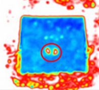
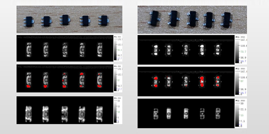
Voids in the chip welding process will cause insufficient heat dissipation during the use of the device, affecting its service life and reliability. Using ultrasonic testing methods, welding void defects can be quickly and effectively identified.
|
|
|
|
|
|
Welding voids |
Warping of silicon wafers |
Bread chips |
Cracks in silicon wafers |
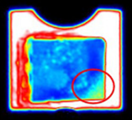
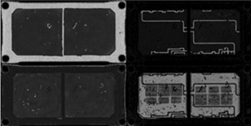
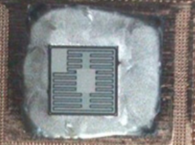
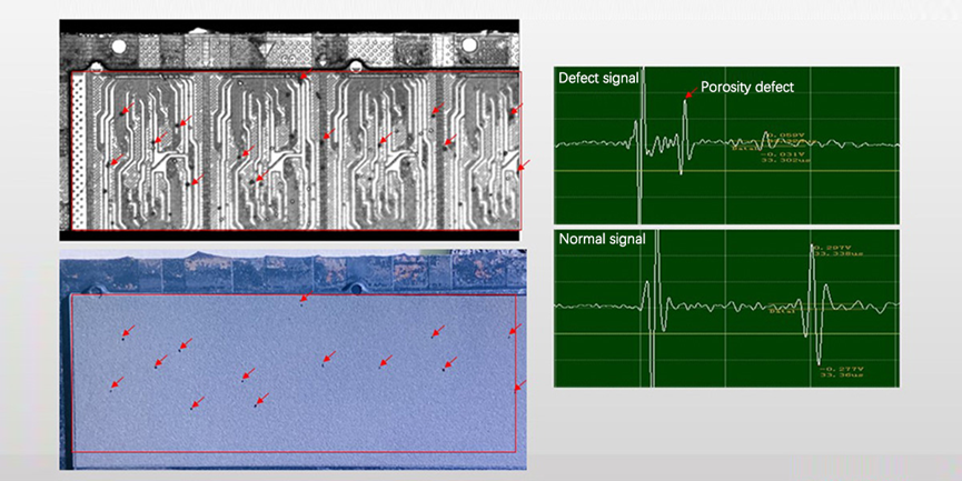
Detection of package delamination defects after the plastic encapsulation process
Ultrasonic scanning phase detection mode to accurately identify delamination defects between resin plastic and metal frame
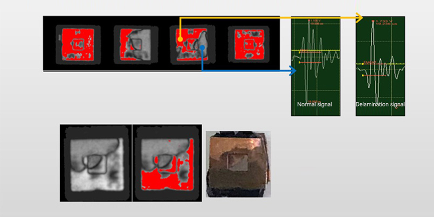
The oxidized area after peeling is basically the same as the red area
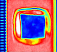
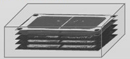
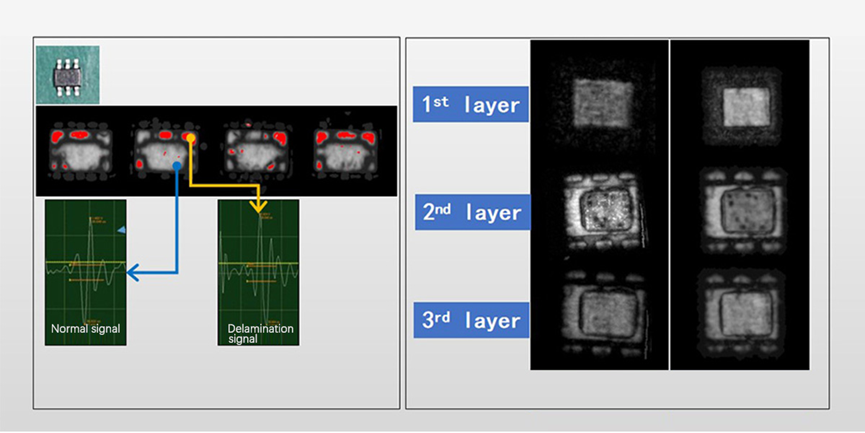
Void detection and multi-layer detection of thinner packages
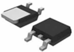
Detection case TO series
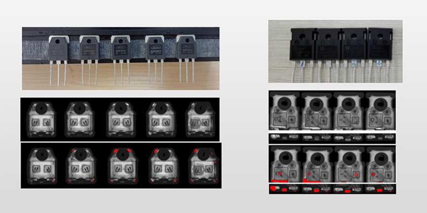
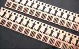
Test the whole board
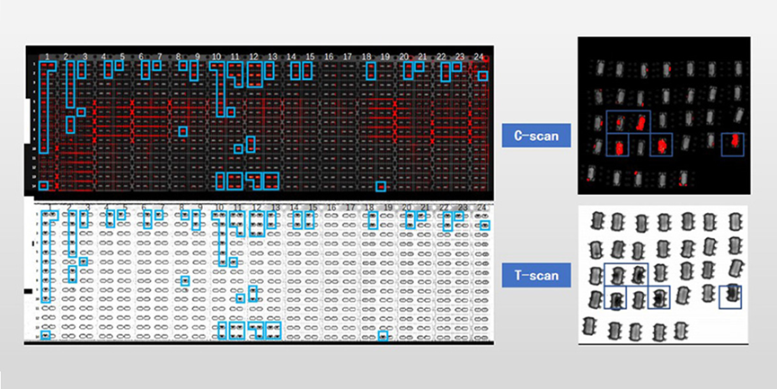
Test a single chip
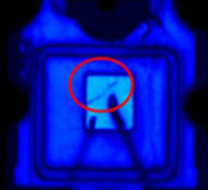
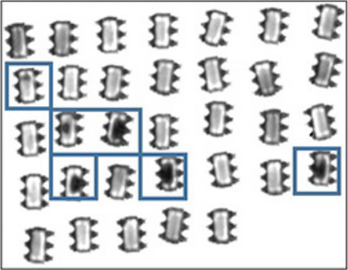
Typical application case: memory chip package pores
Typical application case: memory chip layering defect
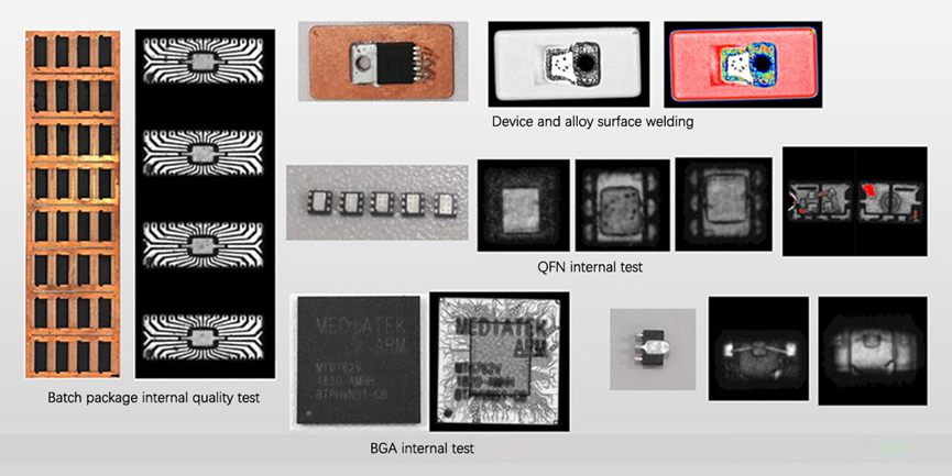
Other test cases
Guangzhou Minder-Hightech Co.,Ltd.
Copyright © Guangzhou Minder-Hightech Co.,Ltd. All Rights Reserved
 EN
EN
 AR
AR
 BG
BG
 CS
CS
 DA
DA
 NL
NL
 FI
FI
 FR
FR
 DE
DE
 EL
EL
 IT
IT
 KO
KO
 NO
NO
 PL
PL
 PT
PT
 RO
RO
 RU
RU
 ES
ES
 SV
SV
 TL
TL
 IW
IW
 ID
ID
 LT
LT
 SR
SR
 SL
SL
 UK
UK
 VI
VI
 ET
ET
 HU
HU
 TH
TH
 TR
TR
 FA
FA
 AF
AF
 MS
MS
 GA
GA
 IS
IS
 HY
HY
 AZ
AZ
 KA
KA