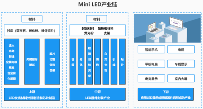
In the LED industry chain, the upstream is the epitaxial manufacturing of LED luminescent materials and chip manufacturing, the midstream is the LED device packaging industry, and the downstream is the industry formed by the application of LED displays or lighting devices.
Developing packaging technologies with low thermal resistance, excellent optical properties, and high reliability is a necessary path for new LEDs to become practical and enter the market.
Packaging is the link between industry and market. Only when packaged well can it become a terminal product and be put into practical application.

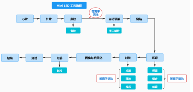
In the packaging process of Mini LED, if there are particle pollutants, oxides, and epoxy resin pollutants on the chip and substrate, it will directly affect the yield of Mini LED products. Plasma cleaning before glue dispensing, lead bonding, and packaging curing during the packaging process can effectively remove these pollutants.
Principles of Plasma Cleaning
Chemical or physical processes are used to treat the surface of an object, achieving molecular level pollutant removal (usually with a thickness of 3-30nm), thereby improving the surface activity of the object.
The pollutants to be removed may include organic matter, epoxy resin, photoresist, oxides, microparticle pollutants, etc.
Corresponding to different pollutants, different cleaning processes should be adopted. Depending on the selected process gas, plasma cleaning can be divided into:
Chemical cleaning: Plasma cleaning, also known as PE, where surface reactions are mainly chemical reactions.
Physical cleaning: Plasma cleaning, also known as sputtering corrosion (SPE), where surface reactions are mainly physical reactions.
Physical and chemical cleaning: Both physical and chemical reactions play important roles in surface reactions.
Mini LED packaging process flow

Application of Plasma Cleaning in Mini LED Packaging Process
In the Mini LED packaging process, different cleaning processes can achieve ideal results for different pollutants and based on the substrate and chip materials. However, using the wrong process gas scheme can lead to poor cleaning results and even product scrapping.
For example, if silver chips are processed using oxygen plasma technology, they may be oxidized, blackened, or even scrapped. In general, particulate pollutants and oxides are cleaned by plasma using a mixture of hydrogen and argon gas. Gold plated material chips can use oxygen plasma to remove organic matter, while silver material chips cannot.
Choosing the appropriate plasma cleaning process in Mini LED packaging can be roughly divided into the following three aspects:
|
Process |
Current situation |
After plasma cleaning |
|
Before applying silver glue |
The pollutants on the substrate can cause the silver adhesive to form spherical shapes, which is not conducive to chip adhesion and can easily cause damage during chip piercing. |
The hydrophilicity of the board is greatly improved, which is conducive to the adsorption of silver glue and chip bonding. At the same time, it can greatly save the use of silver glue and reduce costs. |
|
Wire bonding |
After the chip is pasted onto its board, it undergoes high-temperature curing, and there are pollutants such as oxides on the substrate, which lead to unstable soldering between the chip and the substrate. |
Improve the bonding strength and the tensile strength of the lead wire, thereby increasing the yield rate, |
|
Before packaging and curing |
During the process of injecting epoxy glue into LED, pollutants can lead to high bubble rate, resulting in low product quality and service life. |
Colloidal bonding is more reliable, effectively reducing the formation of bubbles, while also significantly improving heat dissipation and light emission rate. |

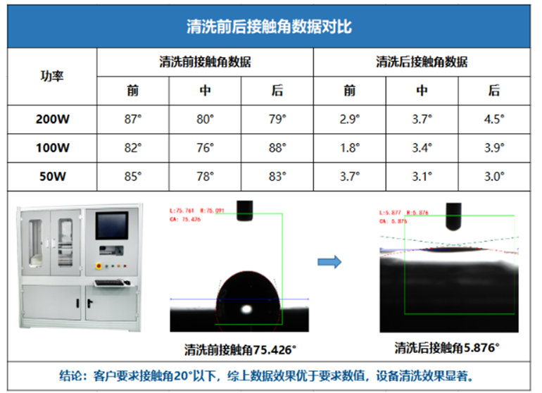
By comparing the contact angle data before and after plasma cleaning, it can be seen that the activation of the material surface, removal of oxides and microparticle pollutants, can be directly demonstrated by the tensile strength and wettability of the bonding leads on the material surface.
Plasma Cleaning Machine
The choice of plasma cleaning in packaging technology depends on the requirements of subsequent processes for the material surface, the characteristics of the material surface, chemical composition, and the properties of pollutants. Plasma cleaning machines can enhance the adhesion, wettability, and reliability of samples, and different processes will use different gases.
Customizable vacuum LED photoresist removal solution
|
Gas |
Surface treatment process |
Application |
|
argon |
Removal of surface dirt |
Pre coating activation, lead bonding, chip bonding of copper lead frames, FBGA |
|
oxygen |
Removal of surface organic matter |
die attach |
|
hydrogen |
Removal of surface oxides |
Lead bonding, chip bonding copper lead frame, FBGA |
|
Carbon tetrafluoride |
Surface etching |
Photoresist removal CSP |
Copyright © Guangzhou Minder-Hightech Co.,Ltd. All Rights Reserved