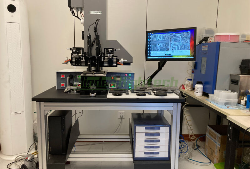
In January 2023, a chip research and development company in Eastern Europe contacted us. They need sample development to verify multiple wafers of different sizes, in order to help more companies upgrade their products.Because it is a preliminary e...
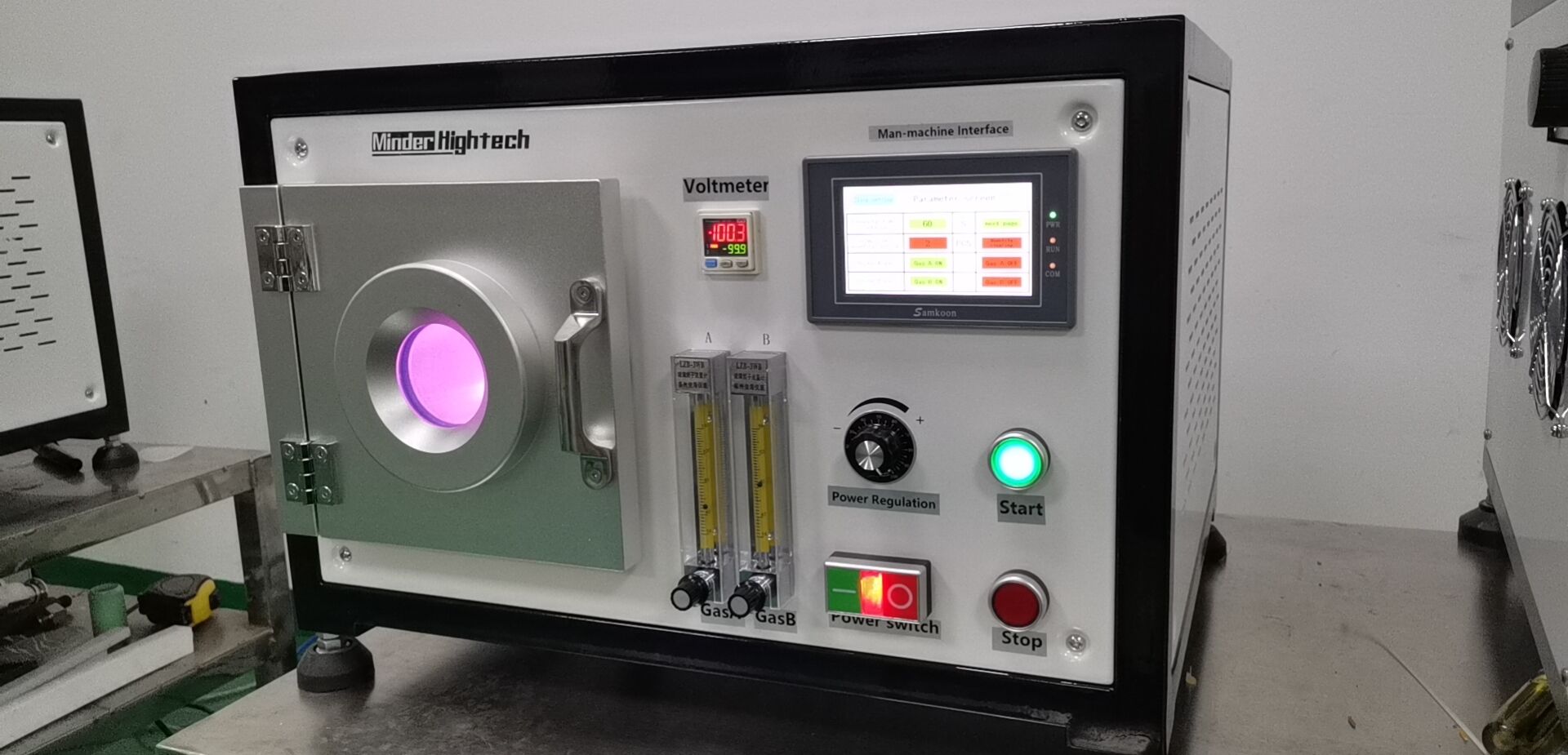
The application of plasma cleaning machines in the semiconductor industry is very extensive, mainly reflected in the following aspects: ▘Surface activation cleaning: For surface activation cleaning of wafers, IC chips, semiconductor silicon wafers, e...
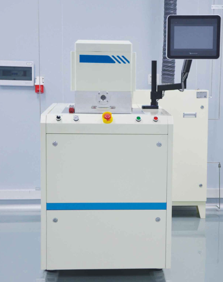
Etching: Two electrodes are available for etching processes: ■ Electrode with wide temperature range (-150°C to +400°C), cooled by liquid nitrogen, liquid circulating refrigerant or variable temperature resistor. Optional purge and liquid exc...
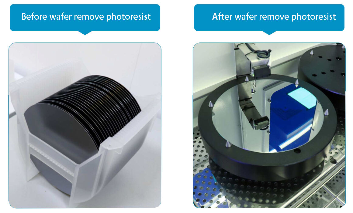
Why is it necessary to remove photoresist? As is well known, photoresist is the core material for semiconductor wafer manufacturing. In the process of wafer manufacturing, photolithography accounts for about 35% of the total wafer manufacturing cost ...

Reactive ion etching system Professionally Provide Customized Solutions for Customers Dual chamber RIE (Cl₂) customization In February 2024, we received a request from a customer for a 100mm wafer Chlorine process. This is an interesting application ...
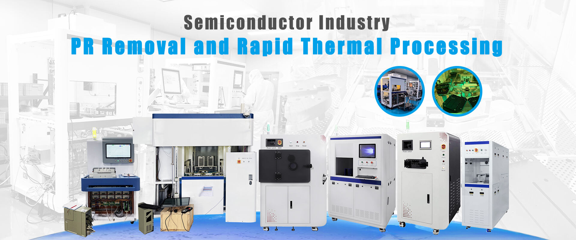
RTP uses halogen infrared lamps as a heat source to rapidly heat up the material to the desired temperature, thereby improving the crystal structure and optoelectronic properties of the material. Its features include high efficiency, energy saving, ...
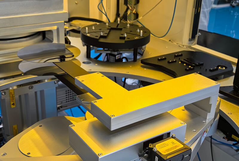
In the LED industry chain, the upstream is the epitaxial manufacturing of LED luminescent materials and chip manufacturing, the midstream is the LED device packaging industry, and the downstream is the industry formed by the application of LED displa...
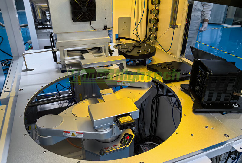
Why remove photoresist? In modern semiconductor production processes, a large amount of photoresist is used to transfer circuit board graphics through the sensitivity and development of the mask and photoresist to the wafer photoresist, forming speci...
Copyright © Guangzhou Minder-Hightech Co.,Ltd. All Rights Reserved